Intel CEO Pat Gelsinger has announced plans to recover the company's chip-making crown by 2025. But the company has shared more details about research that could help it compete even further in the future.
The Santa Clara, California-based company revealed a wide range of new technologies in its pipeline that could keep it from falling further behind on Moore's Law, opening the door to smaller, faster, and cheaper processors with better efficiency. Instead of physically scaling the transistors at the heart of its computer chips, Intel has proposed a way to stack the transistors themselves to pack in more computing resources.
Researchers at Intel outlined the work in papers at the IEDM conference in San Francisco, California.
Intel's core research division, the Components Research Group, is responsible for building out the process andpackaging technologies that help it push the boundaries of Moore's Law. The research division keeps Intel's research and development pipeline full by collaborating with its business units to anticipate future needs and partnering with U.S. research labs, universities, and other chip suppliers, among other groups.
The Components Research division isplaying a central role in Intel's ambitions to retake its leadership in rolling out the most advanced chips, a lead that it has surrendered in recent years to rivals such as TSMC.
RibbonFETs
Intel is trying to strike back against rivals by rearranging the architecture of its transistors. Intel has previously said it plans to upgrade to "gate-all-around"—also known as "nanosheet"—transistors called RibbonFETs in its 20A technology node.
Intel has announced plans to start manufacturing chips with new RibbonFET transistors inside by 2024. The RibbonFETs are based on sheets of current-carrying silicon stacked in a column. Unlike the FinFETs used in the most advanced chips on the market, where the gate is wrapped around a fin-shaped channel on three sides, the ribbon-shaped channels in Intel's RibbonFETs are completely surrounded by the gate.
The three-dimensional shape of the RibbonFET means more current flows during the "on" state and less current to leak from the channel when the transistor is switched "off." The company said that results in better electrostatic control of the transistor and less power leakage, which can sap the final processor's power efficiency. In the end, the RibbonFETs can consume lesspower and run faster and more efficiently.
Another key technology in thepipeline is a backside power delivery system for transistors called PowerVia.

3D CMOS Transistors
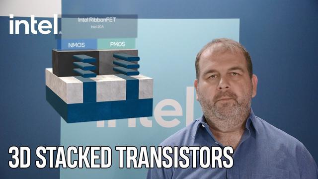
At IEDM 2021, Intel proposed a new process technology where it stacks nanosheet transistors on top of each other to create more room on the chip to squeeze components. Intel said the 3D CMOS transistors would allow it to pack 30% up to 50% more transistors in every square millimeter of silicon in its products.
The most advanced modern processors contain tens of billions of transistors assembled into logic gates, which are in turn arranged into components such as central processors and memory caches. These logic gates are based on billions of pairs of NMOS and PMOS transistors. The MOSFETs are sprawled out side by side on the plane of the chip, with electric current flowing through the interconnects between them.
But stacking the transistors results in a silicon metropolis with everything closer together. That would also reduce the distance that the current must travel from transistor to transistor, increasing power efficiency.
Itcould take years for Intel to improve the 3D CMOS transistors to the point where it would make sense to start mass production. But the 3D transistor technology could give Intel another lever to pull to improve its chips' speed and power efficiency.
"At Intel, the research and innovation necessary for advancing Moore's Law never stop," said Robert Chau, general manager of Intel's Components Research arm, in a statement.
3D Packaging
Intel is also investing in its advanced packaging arsenal to pack more computing power into the same silicon area. The semiconductor giant plans to start rolling out more products by stacking tiny slabs of silicon called "chiplets or "tiles" on top of each other in three dimensions, mixing and matching a wide range of tiles instead of loading everything on a single system on a chip (SoC).
Intel uses its 3D packaging technology called Foveros to stack tiles with direct copper-to-copper bonding of the interconnects relaying data between the tiles. That results in better power efficiency, interconnect density, and signal routing, while limiting heat dissipation. Intel said it can take advantage of Foveros to place interconnects on the underside of a die as close as 50-µm apart.
Intel said its research department is now working on the next generation called Foveros Direct that reduces the gap between the interconnects to less than 10-µm apart.
The company said it is targeting a more than tenfold increase in interconnect density with Foveros Direct. That could reduce the time it takes for data to travel between the tiles in a package, boosting performance.
Intel said its components research armis working on a wide range of new technologies in parallel, related to transistors, packaging, memory, and interconnects as well as quantum computing and new materials. Intel said that it is also researching GaN-based switches for more far efficient on-chip powerdistribution.


