This article discusses the basics of computer chips and focuses on the materials utilized during their fabrication as well as the latest advances in this particular field.
Image Credit: Preechar Bowonkitwanchai/Shutterstock.com
Introduction to Computer Chips
A computer chip is a compact form of electronic circuit, also characterized as an integrated circuit (IC), that is one of the basic units of most electronic equipment, particularly computers. These chips are also referred to as micro-chips. Computer chips are compact and made up of semiconductors, which include multiple tiny elements such as transistors and are used to send electrical data packets. They gained popularity in the latter part of the twentieth century owing to their tiny size, high efficiency, and ease of manufacture.
Fundamental Classification of Computer Chips
There are various fundamental types of such chips, including analog, digitally functional micro-chips, and mixed-signal transmission computer chips. These several classes govern how they send messages and differ in their operational and functional processes. Their categorization substantially affects their performance and compactness, with the digital computer chip being the most compact, highly efficient, most robust, and most extensively employed, transferring data packets as a sequence of ones and zeros.
Which Material is Abundantly Used to Fabricate Computer Chips?
Silicon is abundantly present and is the most utilized substance for the fabrication of computer chips. Silicon is a naturally occurring semiconductor. The injection of imperfections to silicon can change its electrical characteristics, a technique known as doping. Owing to these properties, it is an effective substance for the fabrication of transistors.
The silicon wafers or platforms that serve as the foundation of microchips are composed of silicon, while the metal wires used to connect the sections of circuitry are made of aluminum or copper. Silicon is a vastly occurring semiconductor, which means it transmits or insulates electricity, and typical beach sand has a large concentration of silicon.
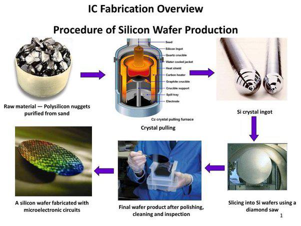
Silicon is cleaned, made molten, and chilled into an ingot before being utilized to produce microchips. The ingots are then cut into 1-millimeter-thick wafers. These wafers are cleaned mirror-smooth before going through a sophisticated procedure to generate chips.
This comprises photolithography, which imprints structures on wafers; ion implantation, which alters the electrical characteristics of silicon in specific locations; etching, which eliminates unnecessary silicon; and transient gate construction. After that, the metal circuitry is attached. Metal circuitry can be found in more than 30 layers on some computer chips. The carbon transistors would be reduced in size, allowing charges to pass with minimal restriction. This would allow the gadgets to turn on and off more quickly.
Limitations
Related Stories
Although silicon might be used extensively for computer chips, owing to certain limitations alternatives are being worked upon. Silicon chips are only economical if they are tiny.

Silicon furnaces are becoming 10 times more expensive every several years. Furthermore, it is hard to reconcile with other elements in a timely and cost-effective manner. Isolated silicon atoms have a physically demanding limit (about 0.2nm), yet their activity becomes unpredictable and hard to sustain under certain conditions. Without the potential to further downsize ICs, silicon cannot continue to produce the benefits it has thus far.
Carbon Nanotube Computer Chips
In 2019, researchers focused on carbon nanotubes for the fabrication of computer microchips as they offer major benefits in terms of energy consumption. Carbon nanotubes are nearly as slender as an atom. They also transport electrical charges substantially well. As a result, they produce superior semiconductor transistors as compared to silicon.
More from AZoM: Tackling the Chip Shortage with the Semiconductor Circular Economy
Carbon nanotube electronics might theoretically be three times better than silicon computer chips in terms of processing speed. They would also use around one-third of the energy that silicon processors use.
Nanomagnetic Computer Chips
Nanomagnet-based computer chips are expected to replace silicon-based computer chips shortly. Nanomagnets employ nanomagnetic technology to convey and process data. They do this by utilizing switchable magnetic modes that are photolithographically adhered to the system networks of a circuit.
Nanomagnetic logic functions similarly to silicon-based semiconductors, except instead of turning transistors on and off to generate binary data, magnetization levels are switched. This binary data may be interpreted via dipole-dipole couplings (the connection among each magnet's north and south poles). Nanomagnetic logic consumes relatively little power since it does not depend on an electrical current. When environmental issues are taken into account, this renders them the appropriate substitute.
Apart from the above-mentioned materials, zeolite thin film micro-chips are also being researched owing to their low dielectric constant and superior efficiency.
Latest Research Advances
The technologies for computer chips integration of 2-D materials have been discussed in the latest research published by David J. Moss. Chip-scale embedded electronics, which have a small footprint, reduced energy requirement, and inexpensive production due to widespread production, have had a significant impact on our modern lifestyles.
Although traditional metal-oxide-semiconductors, such as silicon, have influenced embedded devices, they incur several inherent material restrictions. Other material integrations on-chip has shown to be an appealing method for overcoming these issues.
Since the ground-breaking development of nanoparticles such as graphene, 2D multi-layered materials have piqued the majority's curiosity, and the material category is fast expanding. When compared to bulk counterparts, 2D alternatives have numerous exceptional qualities, including ultra-high charge transport, layered sensitive bandgaps, significant asymmetry, bandwidth, minimal photonic scattering, and outstanding nonlinear absorption characteristics.
Their inherent thin shape further benefits high-density integration and low-power performance. The use of 2D materials on traditional electronic components such as computer chips combines the perfect combination.
The advantageous 2D materials include graphene, graphene oxide, transition metal dichalcogenides, black phosphorus as well as hexagonal boron nitride, Mxenes, perovskites, and metal-organic frameworks. These materials have been used for thin films, microchips, field-effect transistors, micro-supercapacitors, and energy storage materials.
Future of Computer Chips
The shortage of silicon chips has led to a surge in the price of computer components and electronic gadgets involving computer links. Using a revolutionary silicon computer chip technology, we may be able to create quantum computers cheaply and frequently in the future. The University of Melbourne investigated this approach.
The silicon computer chip approach can generate large-scale configurations of numbered particles that can be manipulated and seen for their quantum states to be changed, linked, and read-out. This will allow engineers to design quantum logic functions amongst vast arrays of subatomic particles while maintaining very precise operations throughout the entire system.
References and Further Reading
Innovation News Network, 2022. Advancements in quantum computing with silicon computer chip.[Online] Available at: https://www.innovationnewsnetwork.com/advancements-quantum-computing-silicon-computer-chip/17003/
Moss, David. 2022. Integration technologies for chips with 2D materials. OSF Preprints. Available at: https://osf.io/tqmes/
Nisar, Muhammad Shemyal, et al. 2021. On-Chip integrated photonic devices based on phase change materials. Photonics. 8(6). 205. Multidisciplinary Digital Publishing Institute. 2021. Available at: https://www.mdpi.com/2304-6732/8/6/205
Norton, M. G. 2021. Silicon—The Material of Information. In Ten Materials That Shaped Our World. 177-195. Springer, Cham. https://link.springer.com/book/10.1007/978-3-030-75213-2
Xiang, Shen, et al. 2021. Development Trend of 2D Materials Research Domain Based on National Science Foundation Funded Projects. Science Focus 16(6). 1-15. Available at: 10.15978/j.cnki.1673-5668.202106002
Disclaimer: The views expressed here are those of the author expressed in their private capacity and do not necessarily represent the views of AZoM.com Limited T/A AZoNetwork the owner and operator of this website. This disclaimer forms part of the Terms and conditions of use of this website.


